 |
 |
 |
| Home | News | Research | Group | Publications | Dr. Wang | Books | Patents | Contact |
|
in situ TEM Measurement Technique 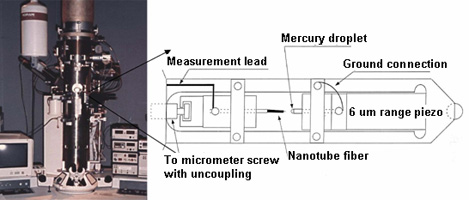 Figure 1. A transmission electron microscope and a schematic diagram of a specimen holder for in-situ measurements To carry out the property measurement of a 1D nanostructure, a specimen holder for an TEM was built for applying a voltage across a 1D nanostructure and its counter electrode (Figure 1). In the area that is loading specimen in conventional TEM, an electromechanical system is built that allows not only the lateral movement of the tip, but also applying a voltage across the 1D nanostructure with the counter electrode. This set up is similar to the integration of scanning probe technique with TEM. The static and dynamic properties of the 1D nanostructures can be obtained by applying a controllable static and alternating electric field. The microstructure of the measured object can be fully characterized by electron imaging, diffraction and chemical analysis techniques. 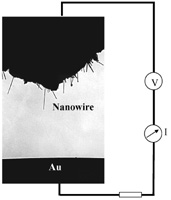 Figure 2. TEM image showing one-dimensional nanostructures at the end of the electrode and the other counter electrode. A constant or alternating voltage can be applied to the two electrodes to induce electrostatic deflection or mechanical resonance. The 1D nanostructure to be used for property measurements is directly imaged under TEM (Figure 2), and electron diffraction patterns and images can be recorded from the 1D nanostructure. The information provided by TEM directly reveals both the surface and the intrinsic structure of the 1D nanostructure. This is a unique advantage over the SPM techniques. The distance from the 1D nanostructure to the counter electrode is controllable. The typical dimensions of the 1D nanostructures are 5 - 100 nm in diameter/width and lengths of 1 - 20 µm. The counter electrode is typically an Au ball of diameter ~ 0.25 mm. Static and dynamic properties of the 1D nanostructures can be obtained by applying controllable static and alternating electric fields. Resonance of carbon nanotubes can be induced by tuning the frequency of the applied voltage. The technique is powerful in a way that it can directly correlate the atomic-scale microstructure of the carbon nanotube with its physical properties, providing a one-to-one correspondence in structure-property characterization. Due to the rectangular cross-section of the nanobelt, two fundamental resonance modes have been observed in corresponding to two orthogonal transverse vibration directions, showing the versatile applications of nanobelts as nanocantilevers and nanoresonators. The bending modulus of the ZnO nanobelts was measured to be ~52 GPa. |
|||